DEDBUG
Next-Gen Deadbug and Free-Form Prototyping Board
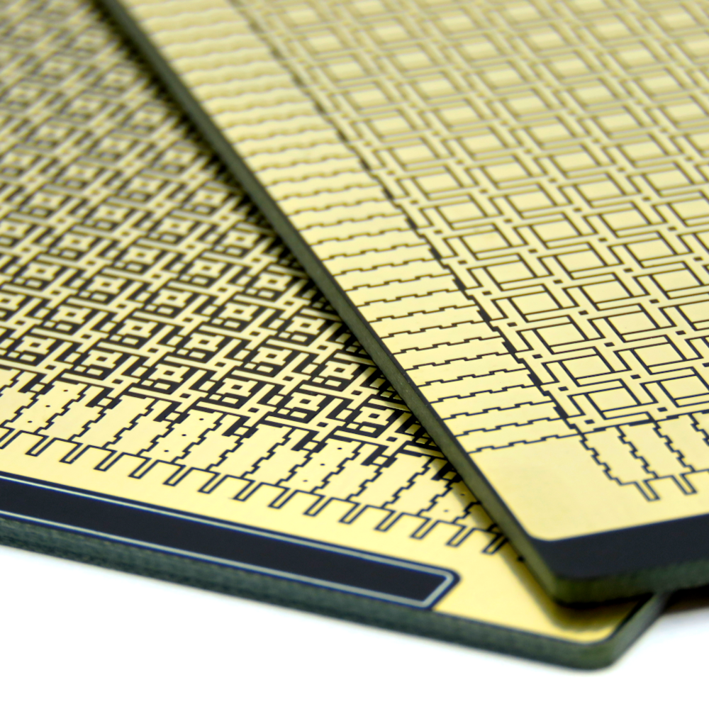
DEDBUG is a prototyping board specifically engineered for deadbug assembly and free-form circuit construction using components reclaimed from electronic waste. In contrast to conventional perfboards and stripboards, its primary purpose is to facilitate the integration of surface-mount devices, rather than through-hole components.
The board's unique layout enables users to experiment with and fabricate arbitrary circuits with minimal effort, illustrating that modest resources suffice to modify and repurpose discarded electronics rather than the costly manufacturing of new hardware.
With the release of version 0.3, the DEDBUG platform has transitioned to a flexible printedcircuit board (Flex PCB), further enhancing its adaptability for unconventional experimentation.
v0.3 Features
- Enhanced adaptability: The platform's upgrade to a Flexible PCB expands the platform's suitability for unconventional experimentation.
- Dual-edge power bus: A dedicated VCC/GND bus runs along the right-hand and bottom edges of the board, providing convenient current distribution.
- Configurable edge connections: The top right corner allows a wire or crocodile clip to be soldered, creating either a VCC or a GND bus on demand.
- Flexible bridging options: Edge pads can be linked to the bus, to adjacent edge pads, or to the central prototyping zone using either solid solder joints or 0402-size zero-ohm resistors, giving the researcher fine-grained control over connectivity.
- Via-based pad pairing: Corresponding edge pads on opposite sides are interconnected through plated-through vias; when one side hosts a VCC bus and the opposite side a GND bus, a single via bridge makes both rails available within the prototyping areas on either side.
- Versatile prototyping region: The central prototyping area supports both traditional wiring using enameled copper wire and wire-free bridging of the cross-shaped pads, accommodating rapid layout iterations.
- Unique SMD component grid: The prototyping grid is dimensioned for the most prevalent two-terminal surface-mount packages—0201, 0402, 0603, 0805, 1206, and 1210. This layout streamlines the assembly of high-density circuits that would otherwise be challenging to hand-solder, and it enables researchers to integrate any salvaged SMD component extracted from electronic waste.
Funding
This project received funding through Constant as part of their Technodisobedience project and NGI0 Entrust, a fund established by NLnet with financial support from the European Commission's Next Generation Internet program. Learn more at the NLnet project page.

